Applications of Nanotechnology and Nanomaterials in Construction: Part Two
Abstract
Due to the small size of nano-materials, their physical / chemical properties (e.g. stability, hardness, conductivity, reactivity, optical sensitivity, melting point, etc.) can be manipulated to improve the overall properties of conventional materials.
Nanoparticles may also assist in the optimization of conventional components like batteries, catalysts, solar cells or fuel cells.
The automotive industry will certainly be influenced by the development and implementation of nanotechnology. Due to the small size of nano-materials, their physical / chemical properties (e.g. stability, hardness, conductivity, reactivity, optical sensitivity, melting point, etc.) can be manipulated to improve the overall properties of conventional materials.
Metal nanoparticles are being considered for potential use in catalytic converters since the catalytic reactivity would be significantly enhanced due to the increased surface area of the metal. Coolants utilize nanoparticles and nano-powders to increase the efficiency of heat transfer and potentially reduce the size of the automotive cooling equipment. Some manufacturers are currently using nano-magnetic fluids in shock absorbers to increase vibration control efficiency. Wear-resistant, hard-surface nano-coatings are being investigated for applications in bearings, cylinders, valves, and other highly stressed components.
High efficiency nano-layers of semiconducting materials provide electronic components and systems with a longer lifetime. Sensors based on nano-layer structures find applications in engine control, airbag, anti-lock brake and electronic stability program systems. Nanoparticles may also assist in the optimization of conventional components like batteries, catalysts, solar cells or fuel cells.
The most promising automotive applications of nanotechnology include the following:
• Improved materials with CNTs, graphene and other nanoparticles/structures
• Improved mechanical, thermal, and appearance properties for plastics
• Coatings & encapsulants for wear and corrosion resistance, permeation barriers, and appearance
• Cooling fluids with improved thermal performance
• Joining interfaces for improved thermal cycle and crack resistance
• Metal alloys with greater mechanical strength
• Metal matrix and ceramics with improved mechanical properties
• Solder materials with crack resistance or lower processing temperatures
• Displays with lower cost and higher performance
• Batteries for electric vehicles and fuel cells with improved energy capacity
• Automotive sensors with nano-sensing elements, nanostructures and nano-machines
• Hybrid electric vehicles using electrical interconnects for high-frequency and high-power applications
• Electrical switching including CNT transistors, quantum transistors, nano-electro-mechanical switches, electronemission amplification, and more efficient solar cells
• tSelf-assembly using fluid carriers.
Nano-fluids are a solid-liquid composite containing nanoparticles with sizes in the 1-100 nm range dispersed and suspended in a liquid. A variety of nanoparticle solids have been used as additives, including metals such as copper and gold, alumina, SiC and CuO ceramics and carbon nano-tubes.
Displays with improved performance and unique features are made possible by nanotechnology. Additionally, lower cost light emission sources, such as lasers are possible in the near future. Display technology, under rapid development for consumer electronic devices and home entertainment systems, is also being pursued for automotive applications. Improved performance, longer life, higher energy efficiency, unique presentation features, reduced package size and innovation become the incentive for implementing this new technology.
It may be possible to develop a solder paste system using nano-sized solder particles (or alloying elements) to take advantage of melting point suppression. This would be a technology enabler for upcoming high-density electronics that are heat sensitive, thereby improving reliability of future electronic systems. One promising application of nano-technology to the soldering process is in the use of nano-reactive foils. These foils are comprised of thousands of alternating nano-scale layers of aluminum and nickel that are placed between the two surfaces to be joined. For instance, a nano-reactive foil is placed between two surfaces to ultimately bond a semiconductor device to a Printed Circuit Board.
When activated with a small amount of energy, the nanoreactive foil rapidly reacts chemically in an exothermic reaction. The energy in the form of released heat, melts the adjacent solder and, in this example, bonds the IC to the substrate. The amount of energy released is directly proportional to the number of Al-Ni layers present in the nano-reactive foil.
Microelectromechanical systems (MEMS), the integration of sensors, actuators and electronics are among the fastest growing areas within microelectronics. This advance has been enabled by the extension of the technology of silicon-based photolithography to mechanical devices with small dimensions (microstructures and micromechanisms), some of which have already found significant industrial applications.
The reach of MEMS is now extending to materials other than silicon, and the scope of applications is proceeding beyond the simple physical regime (e.g. accelerometers and pressure sensors) to chemical and biological sensors. The proliferation of MEMS materials and applications, and the need for materials integration, opens up a host of materials science questions. Likewise, new materials being incorporated into MEMS devices introduce a number of new processing and packaging issues not previously encountered with silicon based technology.
The variety of MEMS devices and applications are increasing continuously and it is certain that nanotechnology will make a great impact on sensor technology in the near future. It will give an opportunity to develop small, inexpensive and highly efficient nanotechnology enabled sensors for different applications, which may offer significant advantages over conventional sensors due to the dramatically enhanced physical effects as a result of using of nanomaterials. It is clear that MEMS technology can improve performance over existing technologies, whilst reducing size, weight, and cost -- three critical factors when considering wide scale deployment.
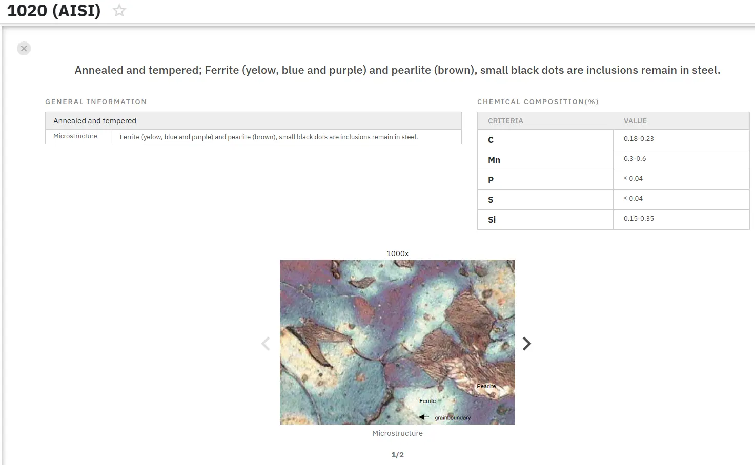
Find Instantly Thousands of Metallography Diagrams!
Total Materia Horizon contains a unique collection of metallography images across a large range of metallic alloys, countries, standards and heat treatments.
Get a FREE test account at Total Materia Horizon and join a community of over 500,000 users from more than 120 countries.